
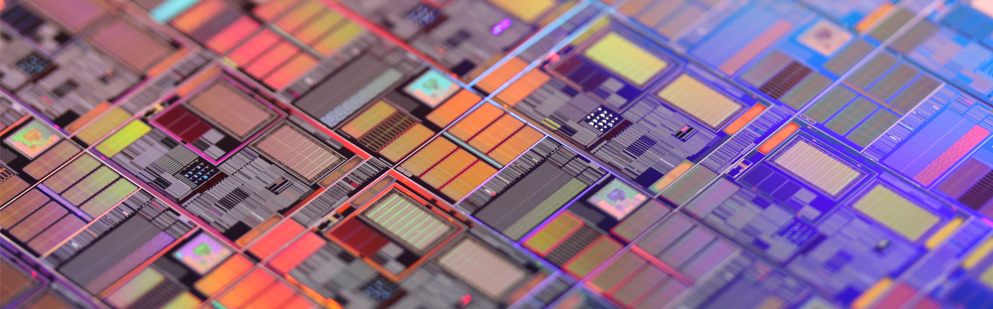
Wafer Services
We provide blank wafer and structured wafer for further processing including advanced metrology.
more info300 mm Wafer Service
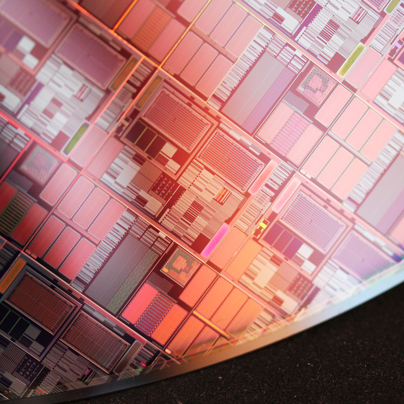
Blank Wafer
300 mm Blank Wafer
Silicon based Layer
- SiO2 (thermal or chemical formed oxide)
- Organo silicate glass (SiCOH/ULK) [porous]
- SiGe
- Doped amorphous Si and poly Si (P, B)
Metals
- PVD: Ta(N), Ti(N), Cu
- CVD: Co
- ECD: Co, Cu
ALD based Oxides and Nitrides
- Al2O3
- HfO2 (doped)
- ZrO2
- More materials upon request
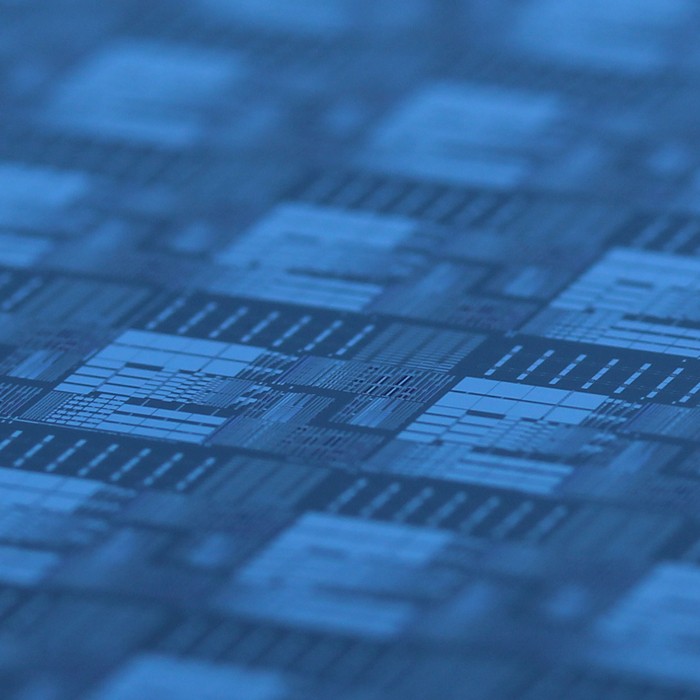
Structured Wafer for CMOS (FEoL/BEoL)
300 mm Structured Wafer
Test Structures for various Processes at ≤ 28 nm Technology Node
- CMP | Plating | Cleaning
- Thin films | STI
Test Structures for functional Layers
- Memory applications
- MIS/MIM structures
Custom Layout Implementation / E-Beam Lithography Nanopatterning
- Complementary Mix & Match
- Small volume series
- more information here!
Test Structures for BEOL / Wafel Level Packaging (IZM-ASSID)
- TSV Test Wafers (via middle, via last)
- Si Interposer with Cu-TSV
- Fine pitch flip Interconnects
- Teships for chip-to-wafer / chip-to-chip / chip-to-substrate bonding
Structured Wafer for Wafel Level Packaging
300 mm Structured Wafer
- TSV Test Wafers (via middle, via last)
- Si Interposer with Cu-TSV
- Fine pitch flip Interconnects
- Testchips for chip-to-wafer / chip-to-chip / chip-to-substrate bonding
Wafer Thinning
- Grinding and polishing of single and compound wafers
- Stress relief etching, Chip-Side-Wall-Healing
- TAIKO wafer processing
Separating
- Mechanical Blade-Dicing, Laser-Grooving
- Laser Stealth-Dicing, Wafer-Edge-Trimming; Circle-Cut
Assembly
- Die to Wafer /Interposer Assembly (Flip Chip soldering)
- Wafer to Wafer temporary and permanent bonding
- Thermo-compression, anodic Wafer Bonding, Hybrid Bonding
High-density and ultra fine Pitch Interconnect Formation
- Galvanic deposition technology
- Solder bumping: SnAg, In, InSn, AuSn, Sn
- Pillar bumping: Cu, Au, Ni, porous nano-gold
- Single-Chip-Bumping on Carrier wafers
- Ultra-Fine-Pitch Bumping < 10µm
TSV Integration
- Front- / Backside TSV
- Cu-TSV liner, full-filled, FS Via-middle, BS Via –Last, Via -First
Metrology
Test wafers are verified in our metrology system park for a fast realization of further qualification steps on site.
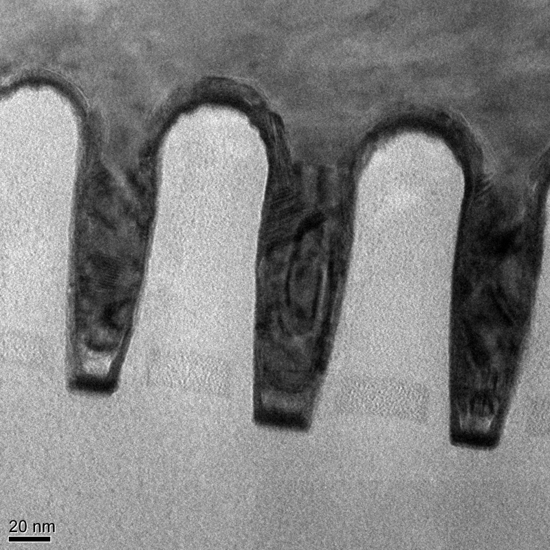
Picture of an EFTEM (Energy filtered transmission electron microscopy)
- Layer thickness and uniformity
- (4-point probing, ellipsometry, XRR, high res. profi lometry)
- Film morphology and structure
- (AFM [3D], XRD, surface inspection, SEM, TEM, porosimetry)
- Chemical composition & contamination
- (ToF-SIMS, XPS, TXRF, REELS, ICP-MS, AAS)
- Patterned defect inspection
- Electrochemical monitoring of electrolyte solutions and additives
- (CVS, LP, EIS, etc.)
- Electrical characterization of functional layers and layer stacks
- (Semi-automatic probing)
Material
Involved Partners
in cooperation with:
