
Creating new products based on 300 mm semiconductor technologies requires significant process development effort and therefore represents a costly and time-consuming challenge. Thus, the availability of 300 mm test wafers and process modules is essential for the development of new critical technology steps and components. Likewise, the supplier industry, which provides tools, raw materials and consumables for the production of silicon microelectronics, can benefit from access to a test environment close to manufacturing conditions in order to qualify new products.
The objective of the Test Wafer Hub project is to provide such a 300 mm test and evaluation platform. The spectrum ranges from suitable test wafers that can be adapted to customer-specific requirements to entire technology modules on established manufacturing equipment including subsequent leading edge characterizations and evaluations.
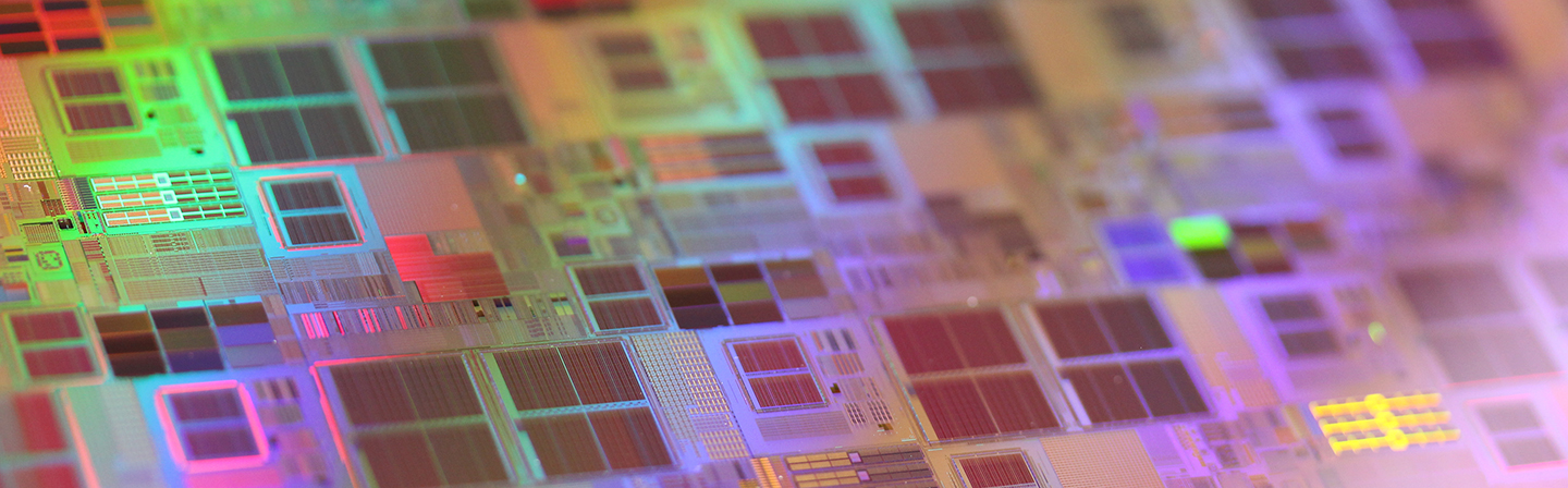
Based on their complementary resources in the areas of process technology development, application-specific know-how and analytics, Fraunhofer IPMS and Fraunhofer IZM-ASSID jointly offer sophisticated structured test vehicles and test substrates for 300 mm CMOS or advanced packaging development. The offering comprises on the one hand front-end-of-line (FEoL) technologies, such as high-k dielectrics and epitaxial Si(Ge) layers, and on the other hand back-end-of-line (BEoL) processes as well as advanced packaging where the metallization, especially by means of copper and its embedding, plays a role.
PROJECT DETAILS:
Concept:
- Supporting customers in process and product development by providing test wafers
- Sharing complementary skills and resources at IZM-ASSID and IPMS
R&D objectives:
- Expanding the portfolio of current test vehicles
- Improved connection of hardware and logistic resources
- Creation of a common marketing platform
Added value:
- Joint offer for process development
- Offering both front-end and back-end technologies through a single point of contact
- Mutual tool backup between partners to improve delivery reliability of products and services
Targeted applications:
- Test wafers for the development of materials and processes for 300 mm silicon fabs
- Material / process screening and development on 300 mm wafers
- Combination of front-end and back-end technologies for reduced development times