 High Performance Center »Functional Integration in Micro- and Nanoelectronics«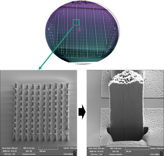
Rising material costs and uncertain supply chains for gold, nickel, and tin-silver alloys are increasing pressure on the electronics and semiconductor industries. This project demonstrates a promising alternative: electroplated aluminum coatings as a high-performance and cost-efficient solution for selected applications.
The focus is on replacing multi-step metallization processes such as Cu/Ni/Au or Cu/SnAg with a single aluminum-based coating process. This approach reduces process complexity, material consumption, and potentially the cost per wafer significantly. It is particularly attractive for cost-sensitive applications such as consumer electronics, household appliances, solar cells, LED lighting, and entry-level automotive applications.
Fraunhofer ENAS has already successfully demonstrated electroplated aluminum coatings on wafers using ionic liquids at laboratory scale and, together with NB-Technologies GmbH, has developed a process chamber for 200 mm wafers. In addition, the bonding capability for fine-pitch aluminum hybrid bonding at temperatures below 300 °C has been demonstrated.
A further innovation step is the use of deep eutectic solvents (DES), promoted by Fraunhofer IST. These solutions are considered more cost-effective and sustainable than ionic liquids and open up new opportunities for industrial implementation.
The objective of the project is to systematically evaluate material properties, bonding performance, and cost potential, and to derive concrete recommendations for industrial deployment. This will establish the foundation for new manufacturing solutions, prototype products, and partnerships within the semiconductor industry.
Objectives
- Reduce costs by replacing Ni/Au/SnAg metallization with a single-step Al-DES-based process (material costs below 30% of the current level).
- Demonstrate industrial readiness through bonding tests below 300 °C and comprehensive material characterization (roughness, purity, porosity).
- Prepare market introduction through wafer cost analysis, material datasheets, and feasibility validation for semiconductor industry partners.